When Smooth Is Never Smooth Enough: The Nanometer-Scale Surface Defects Quietly Destroying Optical Performance
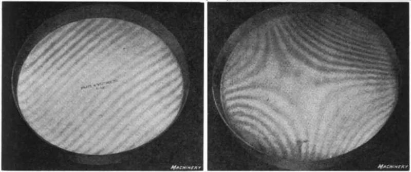
Photo: unknown, probably Franklin D. Jones, Public domain, via Wikimedia Commons
To the unaided eye, a high-quality optical mirror or lens surface appears flawless — a pristine expanse of polished glass or fused silica reflecting light with apparent perfection. But at the scale where photons actually interact with matter, that surface tells a very different story. Peaks and valleys measured in fractions of a nanometer, invisible to any conventional inspection, scatter incoming light in ways that propagate through an entire optical system, degrading contrast, reducing throughput, and in extreme cases, triggering catastrophic thermal damage. For the engineers and physicists designing precision optical instruments, surface roughness is not a cosmetic concern. It is a fundamental physical adversary.
What Roughness Actually Does to Light
The physical relationship between surface texture and scattered light is well established, rooted in electromagnetic scattering theory. When a photon encounters a surface that deviates from a perfect plane, even by a fraction of the wavelength of light, it does not simply reflect as predicted by geometric optics. Instead, energy is redirected into angles that the system designer never intended — a phenomenon known as angle-resolved scatter, or ARS. The severity of this misdirection scales with the ratio of the surface deviation amplitude to the wavelength of the incident light.
This is where the challenge becomes particularly acute at short wavelengths. An optical surface that performs acceptably at 1,550 nanometers — a common telecommunications wavelength — may scatter destructively when illuminated at 193 nanometers, the deep ultraviolet wavelength used in semiconductor lithography. The same physical roughness that is negligible in one application becomes a system-defining flaw in another. As optical systems push toward shorter and shorter wavelengths, the tolerance for surface imperfection contracts accordingly, and the polishing standards that once defined state-of-the-art fabrication become inadequate.
Scattered light does not simply disappear. It redistributes. In an imaging system, scatter produces a diffuse background that reduces contrast — a degradation quantified through the total integrated scatter, or TIS, metric. In a laser cavity or high-power beam delivery system, scattered energy can deposit heat in unintended locations, creating thermal gradients that distort optics and, at sufficient power levels, initiate laser-induced damage. In interferometric metrology systems, where fringe visibility directly encodes measurement precision, even small amounts of scatter introduce noise floors that limit the achievable accuracy of the instrument.
Measuring What Cannot Be Seen
Characterizing surface roughness at the nanometer scale requires instrumentation that is itself a significant engineering achievement. Atomic force microscopy, or AFM, remains the gold standard for quantifying roughness at the sub-nanometer level, using a sharp physical probe to trace the surface topology with sub-angstrom vertical resolution. The resulting data yields roughness parameters — most commonly root-mean-square roughness, or Rq — that describe the statistical distribution of surface height deviations across a measured area.
However, AFM is inherently a contact or near-contact technique, slow to acquire data, and limited in the spatial area it can practically survey. For large optics — the meter-scale mirrors used in astronomical telescopes or the oversized substrates in EUV lithography systems — scanning the entire surface with AFM is impractical. Optical profilometry methods, including phase-shifting interferometry and white-light interferometry, extend coverage to larger areas but sacrifice spatial resolution at the finest scales. Engineers typically combine multiple measurement modalities, assembling what is called a power spectral density, or PSD, curve — a representation of roughness amplitude as a function of spatial frequency across many decades of scale length. The PSD is a more complete descriptor than any single roughness number, because scatter is sensitive not only to the amplitude of surface deviations but to their spatial frequency distribution.
Scatterometry — the direct measurement of angle-resolved scatter from a surface — offers a complementary approach. By illuminating a surface with a known beam and mapping the angular distribution of reflected light, engineers can infer surface roughness characteristics and validate polishing process quality without physically contacting the optic. Commercial scatterometers have become standard equipment in high-end optical fabrication facilities across the United States, enabling rapid feedback during the polishing process.
The Fabrication Challenge: Pushing Toward Atomic Flatness
Reducing surface roughness to levels where scatter becomes negligible — typically below 0.1 nanometers Rq for the most demanding applications — requires polishing processes that operate at the boundary of what is physically achievable. Conventional mechanical polishing, even at its most refined, introduces periodic tool marks and subsurface stress distributions that limit how smooth a surface can become. The industry has consequently developed a range of advanced finishing techniques designed to remove material at the atomic scale without introducing new defects.
Magneto-rheological finishing, or MRF, has become one of the most widely adopted deterministic polishing methods for precision optics. In MRF, a magnetically stiffened fluid ribbon carries abrasive particles across the optical surface in a controlled manner, allowing material removal to be programmed with spatial precision that mechanical tools cannot match. The result is a surface that can be corrected not only for roughness but for low-spatial-frequency figure errors simultaneously.
Ion beam figuring, or IBF, takes a different approach, using a directed beam of ions to sputter material from the surface atom by atom. Because the process introduces no mechanical contact and no polishing compounds, it avoids the subsurface damage and contamination that limit conventional methods. IBF is particularly valuable as a final finishing step for optics destined for extreme ultraviolet or X-ray applications, where the consequences of any residual roughness are severe.
Atomic layer deposition, or ALD, is emerging as a complementary strategy — not for removing material but for filling surface valleys with conformal thin-film coatings at the atomic scale. In certain geometries, particularly for optical coatings applied after polishing, ALD can smooth residual texture in ways that mechanical processes cannot address.
Where the Stakes Are Highest
Three application domains illustrate the real-world consequences of surface roughness with particular clarity. In semiconductor lithography, where EUV light at 13.5 nanometers reflects off multilayer mirrors to pattern features smaller than 10 nanometers on silicon wafers, roughness specifications are measured in fractions of an angstrom. A single mirror with roughness exceeding specification can degrade the aerial image contrast across an entire scanner system, translating directly into yield loss on a production line where wafers carry enormous commercial value.
In high-power laser systems — whether industrial cutting lasers, directed energy platforms, or inertial confinement fusion drivers — surface roughness concentrates optical intensity at scatter sites, creating local hot spots that initiate laser-induced damage at fluences well below the bulk damage threshold of the material. The National Ignition Facility at Lawrence Livermore National Laboratory, for instance, operates with optics fabricated under roughness standards that would have seemed aspirational a generation ago, because the consequence of optical damage at the energies involved is not merely degraded performance but the physical destruction of components.
In precision interferometric metrology — the measurement systems used to calibrate length standards, characterize telescope mirrors, and validate semiconductor wafer flatness — scatter introduces correlated noise that cannot be averaged away. Unlike random noise, which diminishes with repeated measurement, scatter-induced artifacts can be systematic, introducing biases that propagate into measurement results and, ultimately, into the specifications of the products those measurements govern.
A Continuing Refinement
Surface roughness is, in one sense, an ancient problem — humans have been polishing glass since the seventeenth century. But the standards being demanded by contemporary optical systems have transformed it into a frontier challenge, one where the distance between acceptable and unacceptable is measured in atoms rather than micrometers. The tools to characterize roughness at this scale, and the processes to control it, represent some of the most sophisticated manufacturing science in existence. As optical systems continue to push into shorter wavelengths, higher powers, and more demanding precision requirements, the imperative to understand and master scattering at the nanometer scale will only intensify.