The Foundry Gap: Why Integrated Photonics Remains Trapped Outside Silicon's Economic Orbit

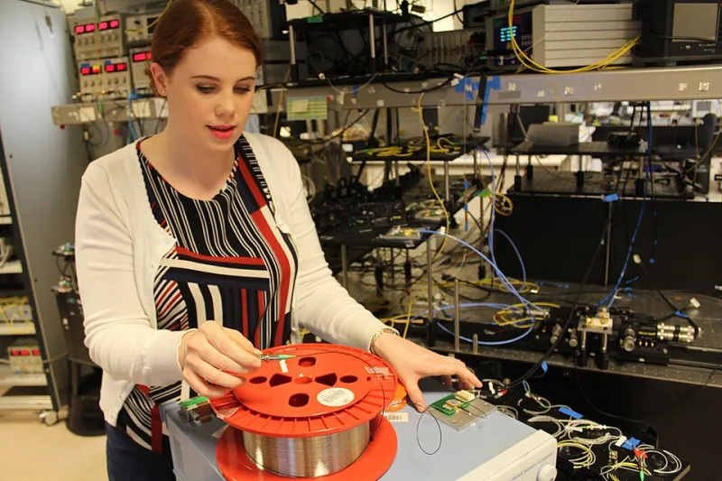
Photo: Planning Commission, GODL-India, via Wikimedia Commons
The semiconductor industry spent fifty years building one of the most formidable manufacturing ecosystems in human history. Standardized process nodes, multi-billion-dollar fabs running at utilization rates above ninety percent, and a global supply chain tuned to produce transistors at vanishingly small cost per unit — these achievements didn't happen by accident. They emerged from decades of iterative refinement, massive capital concentration, and the relentless pressure of a consumer electronics market that demanded ever-cheaper chips.
Integrated photonics has none of that inheritance. And despite hundreds of millions in venture capital, sustained academic interest, and genuine enthusiasm from the datacenter and telecommunications industries, it still doesn't know quite how to acquire it.
A Different Kind of Complexity
To understand why photonics manufacturing remains expensive, it helps to appreciate what makes a photonic integrated circuit, or PIC, fundamentally different from its electronic counterpart. A silicon CMOS chip is, at its core, a precisely patterned arrangement of transistors — structures whose function is largely determined by doping profiles and gate geometry. Photonic circuits, by contrast, must manage the physical behavior of light itself: its wavelength, polarization, phase, and intensity, all simultaneously, across components whose tolerances are measured in nanometers.
A waveguide that is a few nanometers too wide or too narrow changes the effective refractive index of the guided mode, shifting resonant wavelengths and degrading device performance. A coupling gap that drifts slightly across a wafer can render an entire row of devices unusable. These sensitivities aren't engineering failures — they are the unavoidable consequence of working with an electromagnetic wave rather than a flow of electrons. But they make process control dramatically more demanding than what mature CMOS fabs are accustomed to managing.
The result is yield rates that would be considered catastrophic in the semiconductor world. Where a mature logic process might deliver functional die yields above ninety-five percent, photonic foundries frequently operate at yields far below that threshold, particularly for complex multi-component circuits. Every failed die is a wafer area that generated cost but no revenue.
The Chicken-and-Egg Trap
Yield improves with volume. Volume requires customers. Customers require competitive pricing. Competitive pricing requires yield. This circular dependency is not unique to photonics — it has challenged every nascent semiconductor technology — but photonics has proven unusually slow to break out of it.
Part of the problem is market fragmentation. Silicon CMOS achieved scale because it served a single, massive, relatively homogeneous market: digital logic. Photonics, by contrast, serves a constellation of applications — datacom transceivers, LiDAR, quantum information systems, biomedical sensors, optical coherence tomography — each with distinct wavelength requirements, material platforms, and performance specifications. A silicon photonics process optimized for 1550-nanometer telecom applications is not the same process needed for visible-light biosensing or mid-infrared gas detection.
This fragmentation prevents any single process platform from accumulating the volume necessary to drive down costs through learning curve effects. Foundries that serve multiple application segments must maintain multiple process flows, multiplying overhead rather than amortizing it. The economics that made TSMC possible — one dominant process node serving billions of identical devices — simply don't yet exist in photonics.
What the Investment Wave Bought and Didn't Buy
The past decade has seen significant capital flow into photonic integrated circuit companies, from both venture sources and strategic corporate investors. Much of that investment has produced real technical achievements: lower insertion loss, higher integration density, improved coupling efficiency between fiber and chip. The photonic chip available today is meaningfully better than the one available ten years ago.
What the investment has not yet produced is a fundamental restructuring of the manufacturing cost curve. The reasons are instructive. Building a competitive photonic foundry requires not just capital equipment — electron-beam lithography tools, deep-UV steppers, precision etch systems — but also the process recipes, metrology protocols, and engineering expertise to run those tools at high yield, consistently, at scale. That knowledge accumulates slowly. It cannot be purchased outright or replicated quickly, regardless of how much capital is available.
Furthermore, the equipment supply chain for photonics remains thin relative to CMOS. Many of the specialized tools required for photonic fabrication — particularly those needed for III-V compound semiconductor processes used in active components like lasers and modulators — are manufactured in limited quantities by a small number of vendors. Lead times are long, service ecosystems are immature, and the competitive pressure that drives tool cost down in the CMOS world is largely absent.
The Multi-Material Problem
Silicon photonics, the platform most often cited as photonics' best hope for semiconductor-style economics, carries an additional structural complication. Silicon is an excellent waveguide material and a capable modulator platform, but it cannot generate light efficiently. Lasers and amplifiers require direct-bandgap materials — typically indium phosphide or gallium arsenide compounds — that are expensive to process and difficult to integrate monolithically with silicon.
The current industry workaround — heterogeneous integration, in which III-V chips are bonded onto silicon substrates — adds process steps, reduces yield, and increases packaging complexity. It is a pragmatic solution, but it is not an economically elegant one. Until a manufacturable path to efficient on-chip light generation in silicon-compatible materials is demonstrated at scale, photonic circuits will carry a materials integration cost that their electronic counterparts simply do not face.
Paths Forward
None of this is to suggest that photonic manufacturing economics are permanently frozen. Several developments could meaningfully shift the trajectory. The growth of AI-driven optical interconnects in datacenters is creating a volume anchor — a high-unit-count application that could provide the throughput a maturing photonic foundry ecosystem needs. If even a fraction of the projected datacenter optical interconnect demand materializes at the scale analysts are projecting, the resulting volume could drive meaningful yield improvements and process standardization.
Standardization efforts, including multi-project wafer programs run by foundries such as imec and AIM Photonics in the United States, are also attempting to build shared process platforms that allow multiple customers to share wafer runs, spreading fixed costs across more revenue. These programs have grown substantially in recent years and represent a genuine effort to replicate, at smaller scale, the shared-infrastructure model that enabled early CMOS ecosystem development.
Advances in process simulation and machine learning-assisted design for manufacturability may also help close the yield gap faster than purely empirical learning curves would allow, by predicting failure modes before they appear in fabricated devices.
A Long Horizon
The honest assessment is that integrated photonics is not on the verge of achieving semiconductor-style manufacturing economics. The technical and structural barriers are real, and they will not dissolve quickly. What is achievable in the near term is incremental improvement — higher yields, better process control, modest cost reduction — driven by the volume growth that datacom and AI applications may provide.
True cost parity with mature silicon manufacturing, if it arrives at all, is likely a decade or more away, contingent on sustained demand, continued foundry investment, and solutions to the materials integration problem that do not yet exist in manufacturable form. For engineers, investors, and institutions working in this space, clarity about that timeline is not pessimism — it is the precondition for making sound decisions about where to place effort and capital.